
Shanghai Aishengna immersion DUV tools advance chip manufact
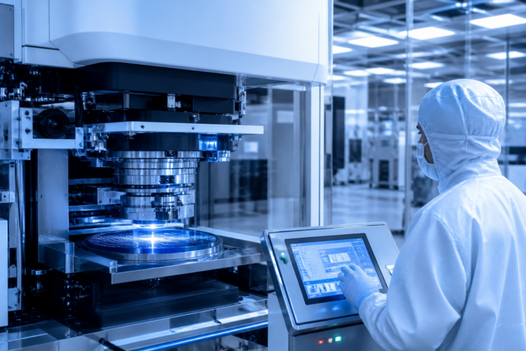
Shanghai Aishengna immersion DUV tools is the focus of this technology-news update.
Shanghai Aishengna Named as the Maker of China’s First Domestic Immersion DUV Chipmaking Tools — First Viable Domestic 7nm-Capable Scanner to be Completed by 2038
In a significant development for China’s semiconductor ambitions, Shanghai Aishengna has been identified as the developer of the country’s first domestic immersion deep ultraviolet (DUV) lithography tools. This milestone marks an important step toward achieving self-reliance in chipmaking equipment. According to a recent report, the project aims to deliver China’s first viable 7nm-capable immersion DUV scanner by 2038. The announcement highlights China’s continued efforts to reduce dependence on foreign semiconductor technology amid rising global supply chain tensions.
The development of Shanghai Aishengna’s immersion DUV tools represents a crucial move to enable Chinese semiconductor manufacturers to produce more advanced nodes domestically. Immersion DUV lithography is an essential technology for fabricating chips at the 7nm process node and beyond, a market segment traditionally dominated by foreign suppliers such as ASML. The emergence of a homegrown solution could reshape China’s chipmaking industry over the coming decade.
Details of Shanghai Aishengna’s Domestic Immersion DUV Project
An unnamed source cited in a recent industry report states that Shanghai Aishengna is responsible for developing China’s first immersion DUV lithography tools capable of supporting 7nm chip production. The company, together with shareholders including Shanghai Micro Electronics Equipment (SMEE) group and Yuliangsheng, has not publicly confirmed these details, and no official statements have been issued.
The project is ambitious, targeting completion of a functional immersion DUV scanner by 2038. This extended timeline reflects a long-term strategic investment, acknowledging the complex, multi-year nature of lithography tool development. The initiative will likely involve incremental milestones focused on addressing the significant technical challenges inherent in immersion lithography technology.
What Is Immersion DUV Lithography and Why Does It Matter?
Immersion DUV lithography is an advanced photolithography technique that uses deep ultraviolet light with a wavelength of approximately 193 nm. It incorporates a thin liquid layer—typically water—between the lens and the wafer to enhance resolution beyond what dry lithography can achieve. This technology is critical for manufacturing semiconductor nodes at 7nm and smaller, where feature sizes approach the physical limits of light diffraction.
Currently, immersion DUV lithography tools are supplied primarily by a few international companies, with ASML leading the market. China’s efforts to develop domestic immersion DUV tools through Shanghai Aishengna aim to close a key gap in its semiconductor manufacturing supply chain, reducing reliance on foreign equipment that is often subject to export restrictions.
Technical Capabilities and Challenges of the Domestic Immersion DUV Scanner
The reported Shanghai Aishengna immersion DUV tools are designed to enable semiconductor fabrication at the 7nm process node, a benchmark of advanced manufacturing. Achieving this requires precise optical systems, high-quality light sources, and sophisticated mechanics and control software to maintain nanometer-scale accuracy during wafer exposure.
– Capabilities: The scanner is expected to support immersion lithography techniques that deliver higher resolution and throughput suitable for 7nm chip production.
– Comparison with international tools: While international immersion DUV systems have been refined over many years, Shanghai Aishengna’s tools represent China’s first viable effort, with performance anticipated to improve over time.
– Development challenges: Significant hurdles include mastering complex optical engineering, achieving required reliability and yield, integrating advanced light sources, and overcoming material and manufacturing constraints.
These challenges explain the extended development timeline through 2038, underscoring the scale of innovation required to produce a competitive immersion DUV scanner.
Impact on China’s Semiconductor Industry and the Global Ecosystem
The introduction of Shanghai Aishengna immersion DUV tools would have several important implications:
– Supply chain independence: Developing domestic immersion DUV equipment reduces China’s vulnerability to foreign export controls that currently limit access to advanced lithography tools.
– Support for local fabs: Chinese semiconductor manufacturers targeting 7nm and potentially more advanced nodes would gain improved access to critical manufacturing equipment, accelerating technology advancement.
– Global competition: A successful domestic tool could alter competitive dynamics in the semiconductor equipment market and chip manufacturing, potentially challenging the dominance of existing suppliers.
However, this development does not immediately disrupt the global market; the path to mass production and widespread adoption remains lengthy and uncertain.
China’s Semiconductor Equipment Landscape: Context and Comparisons
China’s semiconductor equipment sector has historically depended heavily on foreign technology, particularly from European and Japanese suppliers. ASML’s immersion DUV scanners are considered the industry standard for advanced lithography. Domestic Chinese lithography efforts have largely focused on less advanced dry DUV systems, with limited success in matching international capabilities.
Shanghai Aishengna’s reported breakthrough represents the most ambitious domestic push into immersion DUV technology to date. It aligns with China’s broader strategic goal of semiconductor self-sufficiency amid geopolitical and trade tensions restricting access to critical technologies.
Limitations and Remaining Unknowns
Despite the promising nature of this development, several uncertainties remain:
– Technological gaps: Achieving full 7nm production readiness involves more than lithography tools; other process technologies and ecosystem elements must also mature.
– Production and commercialization: Scaling from prototype to mass production scanners that meet industry standards presents a substantial challenge.
– International market and export controls: The global reception of this technology and the impact of export restrictions on its deployment remain unclear.
The absence of official confirmation from Shanghai Aishengna or its affiliates leaves some details speculative. The long timeline indicates this is a foundational advancement rather than an immediate breakthrough.
What to Expect Next: Milestones and Industry Outlook Toward 2038
Looking forward, Shanghai Aishengna’s immersion DUV project is expected to progress through several phases:
– Research and development: Ongoing refinement of optical, mechanical, and control systems, including prototype testing.
– Pilot production: Small-scale manufacturing and validation in partnership with domestic chipmakers.
– Industrial deployment: Gradual introduction into semiconductor fabs targeting 7nm production nodes.
If successful, this effort could significantly strengthen China’s semiconductor manufacturing ecosystem by 2038, fostering greater technological independence and potentially influencing global equipment markets. Industry observers should monitor official announcements and technical disclosures to better assess project progress and impact.
Key Takeaways
– Shanghai Aishengna immersion DUV tools represent China’s first domestic effort to develop 7nm-capable immersion lithography scanners.
– The project aims for completion by 2038, reflecting a long-term strategic commitment amid complex technical challenges.
– Successful development would reduce reliance on foreign lithography equipment, supporting China’s semiconductor self-sufficiency goals.
– Uncertainties remain regarding commercial viability, production scale, and international market acceptance.
– This initiative reflects China’s broader push into advanced semiconductor technologies amid ongoing global supply chain tensions.
As the semiconductor industry evolves, Shanghai Aishengna’s progress will serve as a key indicator of China’s capacity to produce critical chipmaking equipment domestically. Stakeholders should watch for future updates and official confirmations to understand how this development may influence both domestic manufacturing capabilities and the global semiconductor landscape.
Frequently Asked Questions
What is Shanghai Aishengna's recent achievement in chipmaking technology?
Shanghai Aishengna has been named as the maker of China's first domestic immersion deep ultraviolet (DUV) lithography tools, marking a significant milestone in the country's semiconductor manufacturing capabilities.
What is the significance of the first viable domestic 7nm-capable scanner?
The first viable domestic 7nm-capable scanner is crucial because it enables China to produce advanced semiconductor chips at the 7-nanometer process node using homegrown equipment, reducing reliance on foreign technology.
When is the first viable domestic 7nm-capable scanner expected to be completed?
The first viable domestic 7nm-capable immersion DUV scanner is projected to be completed by the year 2038.
How will this development impact China's semiconductor industry?
This development will enhance China's self-sufficiency in semiconductor manufacturing, potentially accelerating domestic chip production and supporting the growth of local technology companies.
Are there any known limitations or challenges associated with the domestic 7nm-capable scanner?
While the domestic scanner represents progress, it is expected to face challenges such as catching up with the performance and precision of leading international lithography tools, and the long timeline until full deployment.
Source: Original reporting

Leave a Reply